American-Made Semiconductors You Can Count On
From prototype development to flexible volume manufacturing, we have the tailored semiconductor manufacturing services you need for a rapid run to market. If you value high-quality ‘Made-in-America’ products that are capable of withstanding the most extreme applications, Polar is the semiconductor foundry for you.
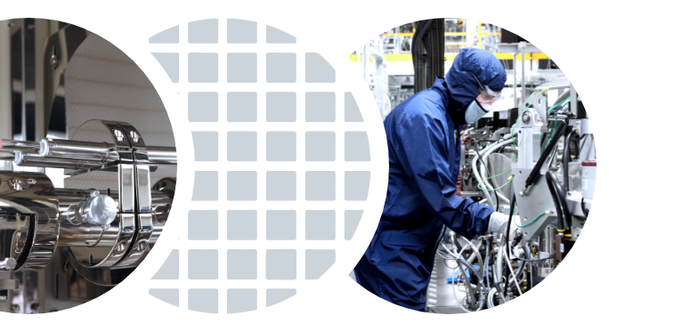
About Our Silicon Wafer Manufacturing Facility
Polar’s semiconductor manufacturing facilities operate with state-of-the-art automation and redundant production support systems to manufacture IC (BCD, BiCMOS) and Discrete (MOS, IGBT) 8-inch silicon wafers for the Power and Sensor markets. With a production capacity of up to 21,000 wafers per month, our silicon wafer manufacturing facility meets all ISO 14644-1 cleanroom standards.
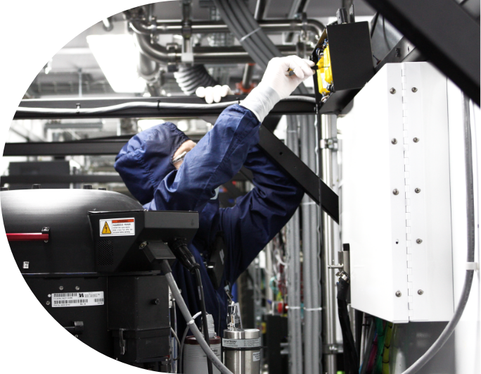
Advanced Semiconductor Manufacturing
Polar’s advanced semiconductor engineering utilizes cutting-edge tools to deliver high-voltage semiconductors with secure, repeatable, and cost-effective chip designs that meet all customer requirements.
- High temp diffusion
- EPI
- High AR trench
- Trench fill (SACVD)
- ALD
- CMP
- Thick metal top
- Thick nitride
- PBO
- Backgrind & backmetal
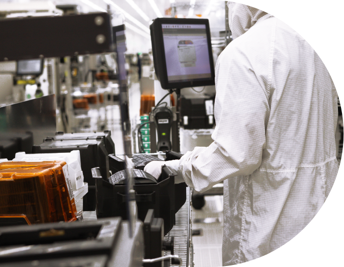
Fab Operation Systems

NetVision
Automate your planning and workflows with Polar’s homegrown Manufacturing Execution System (MES).
- Barcode WIP tracking
- Automatic recipe selection
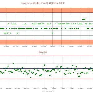
- Real-time SPC
- Automatic shutdown
- PM scheduler

FPS
Stay on top of your equipment and tool state at all times with our intelligent WIP scheduling system.
- Setup, batching, queue timer, reticle management
- Factory dashboard and reporting
- Smart dispatching with visual cues
- Cycle time analysis
- Developed by Inficon

FabGuard
Take Fault Detection and Classification (FDC) tool monitoring and process fingerprinting to the next level.
- Independent tool control
- Process/recipe monitor
- Process shutdown
- Developed by Inficon

Robotic Wafer Transport
Minimize the risk of human error and contamination with our state-of-the-art OMRON wafer delivery robots.
- Increased efficiency
- Improved delivery and CT
- Lot tracker integration
- Minimum operator interaction
Gain Multi-Level Control Through Our Defect Reduction Program
Ongoing fab environment, equipment, process, wafer monitoring, and other improvements.
Environment level
• Paperless
• Airborne particle monitoring
• Temperature & humidity control
Machine level
• FabGuard (FDC)
• Contamination control (TXRF)
• Charge measurement (FAaST)
• Defect monitoring (SP1)
Process level
• Thickness, CD, Overlay Metrology, and SPC
Parametric level
• Screening parameters
• Critical parameters
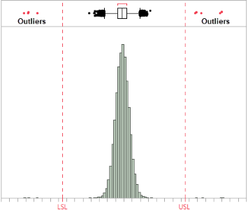
• Outlier screening
• Zero Defect Parameters for automotive
Die level
•Altair, AIT, and TopCon particle inking for Zero Defect Program
Wafer level
• Guardband “Smart” Inking

Semiconductor Manufacturing Equipment
- ASML I-Line Steppers & DUV Scanners
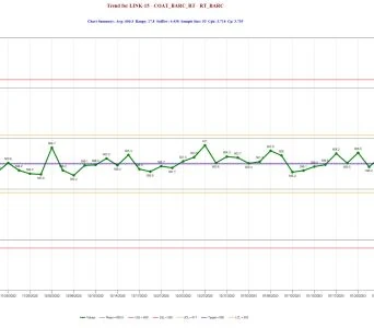
- LINK-ed TEL Coat & Develop Tracks
- ASM & AMAT EPI Reactors
- AXCELIS & AMAT Implanters
- AMAT Mirra CMP KLA
- Automotive Defect Inspection

Other Installed Tools
- TEL-FSI Mercury Spray Tools
- AKRION Wet Benches
- MRL Horizontal Furnaces
- TEL Vertical Furnaces
- TEL LPCVD
- Novellus CVD
- AMAT Dry Etch
- AMAT Endura PVD
- DISCO Grind
- Eclipse Back Metal