World Class American-Made Power and Sensor Semiconductors
Polar is building on decades of experience in high voltage power semiconductor manufacturing with an aggressive capacity expansion and facility modernization. Let’s partner to create your differentiated products.
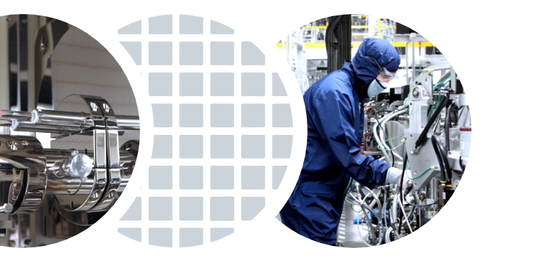
About Our Silicon Wafer Manufacturing Facility
State-of-the-Art Manufacturing
Polar’s semiconductor manufacturing facilities operate with state-of-the-art equipment, automation, and production support systems to manufacture advanced BCD, MOSFET, IGBT, BiCMOS, BiPolar, MEMS, and GaN 8-inch silicon wafers for the Power and Sensor markets.

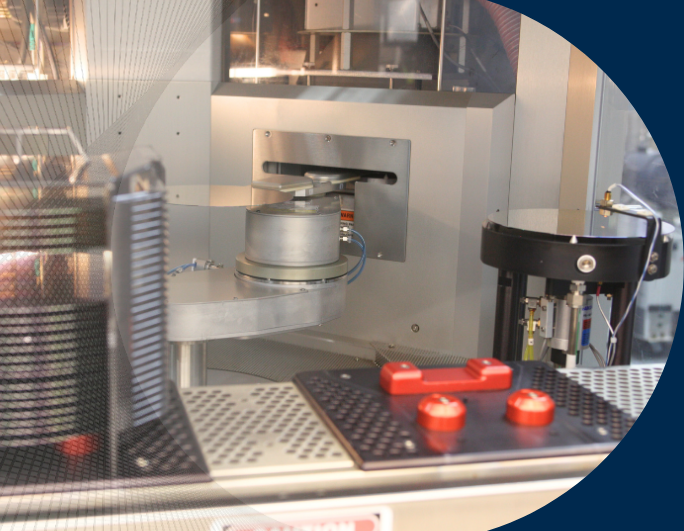
Class 1 Clean Room
With a production capacity of up to 21,000 (IC + discrete mix) wafers per month, our zero-defect-capable silicon wafer manufacturing facility meets all ISO 14644-1 cleanroom standards. In addition, 100% of Polar’s campus is powered by renewable energy.
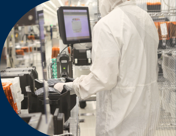
Fab Operation Systems
- NetVision: Polar’s Manufacturing Execution System (MES) for automated planning and workflows
- FabGuard: Inficon Fault Detection and Classification (FDC) tool monitoring
- Robotic Wafer Transport: State-of-the-art OMRON wafer delivery robots minimize the risk of human error and contamination
Expansion and Modernization Project
With full deployment in 2027, Polar is increasing 8-inch production capacity to 40,000 (IC + discrete) or 70,000 discrete wafers per month. To enable and complement the capacity expansion, a large-scale factory automation project is under implementation. This includes Intellion LotTrack to modernize the tracking of carriers, Intellion DisTag RFID lot tracking, Muratec Overhead Transport Systems, and INFICON Intelligent Manufacturing Systems. Additionally, to support national security for Aerospace and Defense applications, Polar is implementing an ITAR compliance program, with future plans to support Trusted Programs.
Process Equipment & Tool Capabilities
Polar’s advanced semiconductor engineering utilizes cutting-edge tools to deliver high-voltage semiconductors with secure, repeatable, and cost-effective chip designs that meet all customer requirements.
| Process | Capabilities |
| Wafer |
|
|
Implant/Diffusion |
|
| Deposition |
|
| Lithography |
|
| Etch |
|
| Metrology |
|
|
Design Enablement |
|
|
Wafer Test |
|
|
Backside Process |
|
|
Analytical Services |
|
Gain Multi-Level Control Through Our Defect Reduction Program
Ongoing fab environment, equipment, process, wafer monitoring, and other improvements.
Environment level
• Paperless
• Airborne particle monitoring
• Temperature & humidity control
Machine level
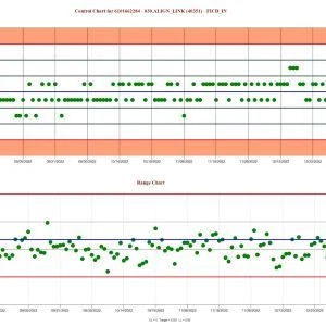
• FabGuard (FDC)
• Contamination control (TXRF)
• Charge measurement (FAaST)
• Defect monitoring (SP1)
Process level
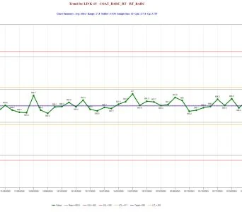
• Thickness, CD, Overlay Metrology, and SPC
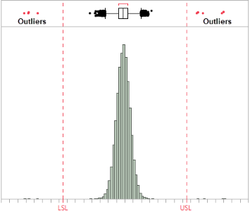
Parametric level
• Screening parameters
• Critical parameters
• Outlier screening
• Zero Defect Parameters for automotive
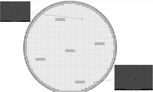
Die level
• Altair particle inking for Zero Defect Program